Posted By: Robert Nickels (ranickels) Posted: 06/06/2020 Technical 06/06/2020 |
Class E Notesthe result of experiments with high efficiency class E amplifiers |
|||||||||||||||||||||||||
|
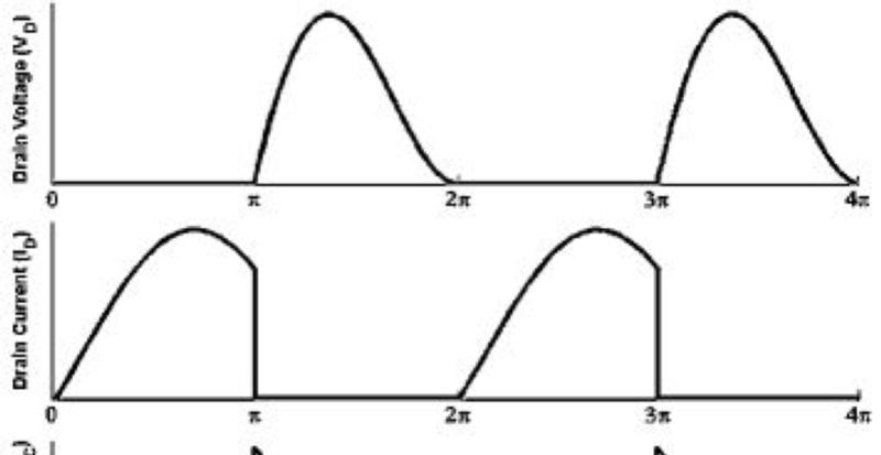
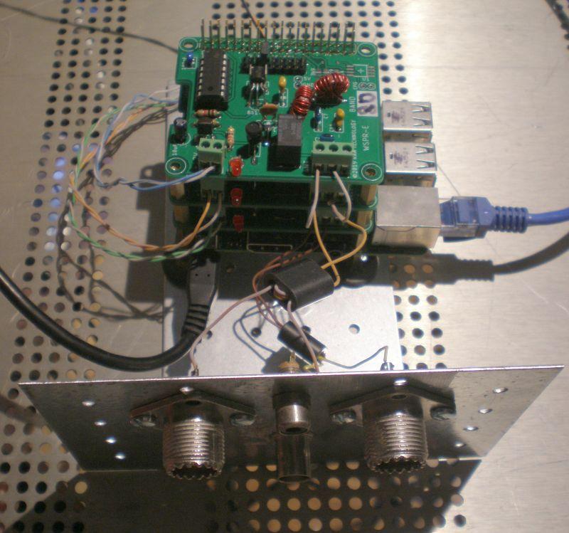
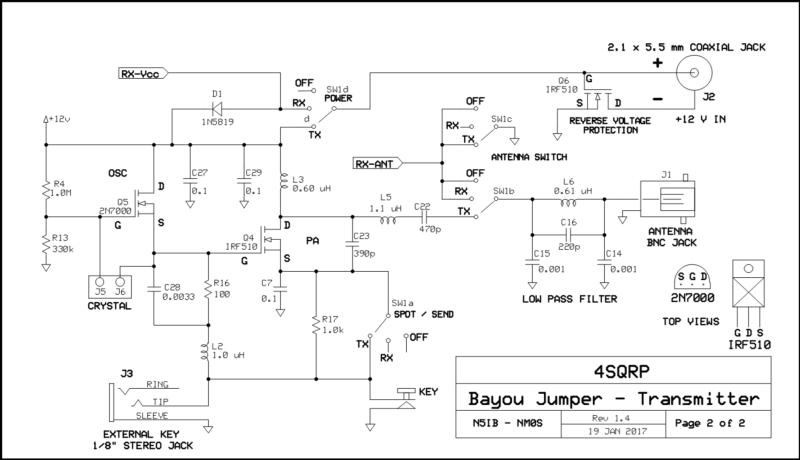
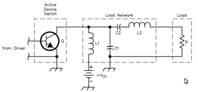
There is a lot of misunderstanding about how a Class E amplifier works. As the result of studying the literature and experimenting, I thought I'd share what I have learned over the past several years. Below is an example of a test amplifier I used to optimize my 2 watt wspr transmitter boards. It can be visualized as two circuits - the amplifier itself and an impedance matching section. The amplifier consists of the swtich (NMOS FET), a parallel capacitor, and a series tuned circut. The shunt (parallel) capacitor adds to the Coss capacitance of the FET as part of the tuned circuit, but also acts to limit the voltage across the FET when it is turned off, and to widen the off-time waveform. The value is not super-critical but it must be capable of withstanding at least 3.5X the drain voltage and should be mounted as close as physically possible to the FET (ideally right across the leads) because inductance here will add harmonics to the output. The fundamental issue with all class E designs is that while NMOS FETs make nearly ideal switches, the gate structure is basically a capacitor, and the higher the power capability, the larger the gate capacitance becomes, and as the nice square edges of the drive signal are rounded off, the less efficient the switch becomes. Fortunately this issue is manageable with the devices used at QRP power levels where digital logic ICs (especially the 74AC family) can do the job. There are many low-side FET driver ICs on the market that work great for power supplies, but sadly most of them are not fast enough for RF. Contrary to intuition, the series network is not made resonant at the operating frequency, and is slightly reactive (resonates lower in frequency). This is because the goal when optimizing a class E amplifier is to minimize the time when the voltage and current across the switch (FET) are both high. Graphically, an ideal class E drain waveform has several key characteristics that are described in the inventor's paper, but which look like the attached "Ideal waveform" photo. In my experience (and verified by more seasoned class E designers), formulas and design aids get you in the ballpark, but simulation (I use ltspice) and actual lab testing are required to arrive at an efficient optimized design where efficiency even greater than 90% are achieved. As proof of this, the experimenter will soon discover that the answers provided by various online and downloadable class E design aids do not always agree. However I will list several here with the usual advice that "YMMV": WAØITP downloadable class E spreadsheet Tonne Software downloadable ClassE design aid NU2B downloadable design tools (DOS and xls) And for those who wish to go straight to the source, the design equations can be found in the inventor, Nathan Sokal's article "Class E Power Amplifiers" in QEX for Jan-Feb 2001. Further information can be found in research papers and in US Patent No. 3,919,656 that he and his son obtained in 1975. This article is copyright by ARRL so is not included here but may be found online LINK
The WAØITP spreadsheet has always produced "good ballpark" efficiency for me by using nearest standard values to those specified by the spreadsheet and is my recommended best choice of design tools. This tool calculates the values fo Dave Cripe's design which has been proven in many applications. However you get there, the bottom line is: if you don't have this waveform, you don't have class E. The design process involves tweaking and adjusting to optimize the drain waveform, because that is the heart of the efficiency of the class E design. Ohms Law tells us, P=E*I, so minimizing E and I means the amount of power dissipated in the transistor is minimized. A typical optimized class E amplifier will be able to convert at least 80% of input power into RF, i.e.. 80% efficiency. That is compared with 50-60% for a class C amplifier, and as high as 90% is possible. The problem is, the output impedance of most class E amplifiers is not 50 ohms, and because of the square wave switching, harmonics are present - the 2nd harmonic is usually the strongest by far. Thus an impedance matching stage is required, and a harmonic filter. The circuit below accomplished both with the fewest parts: 
Related ImagesClick on the image title or on the image itself to open the full-sized image in a separate window.
Related File Attachments
Latest Articles
| ||||||||||||||||||||||||||